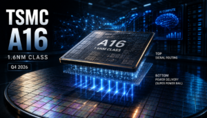
Taiwan Semiconductor Manufacturing Company (TSMC) has reportedly completed the development and verification of its next-generation A16 semiconductor process, commonly described as a 1.6nm-class technology, bringing the world’s largest contract chipmaker closer to mass production of its next major process node.
The A16 technology is designed to deliver improvements in performance, power efficiency and transistor density compared with TSMC’s enhanced 2nm N2P process.
Current reporting from Taiwanese media says TSMC has completed final development and verification of A16, with mass production expected to begin in the fourth quarter of 2026. TSMC itself has previously stated that A16 would be production-ready in the second half of 2026.
The technology is particularly aimed at artificial intelligence and high-performance computing (HPC) applications, where performance and power efficiency are becoming increasingly important.
TSMC’s A16 Moves Beyond 2nm
The A16 represents the next step in TSMC’s advanced-node roadmap after its N2 and N2P technologies.
While the industry is currently moving toward widespread 2nm-class manufacturing, TSMC is already preparing its next-generation process for high-performance computing applications.
The company describes A16 as a technology that combines nanosheet transistors with an innovative backside power-delivery architecture.
What Does 1.6nm Actually Mean?
The term “1.6nm” refers to the technology generation rather than necessarily meaning that every physical feature on the chip measures exactly 1.6 nanometers.
TSMC calls the technology A16, with the “A” referring to the angstrom era of semiconductor scaling.
The industry increasingly uses angstrom-class naming for advanced processes below the traditional 2nm generation.
The Biggest A16 Innovation: Backside Power Delivery
One of the most important changes in A16 is the use of a backside power rail.
Traditional chips deliver power through wiring on the front side of the wafer.
A16 moves the power-delivery network to the backside.
This frees more space on the front side for signal routing.
What Is Super Power Rail?
TSMC calls its backside power technology Super Power Rail (SPR).
The architecture separates power delivery from signal routing.
That can reduce congestion and allow designers to use the front side of the chip more efficiently.
TSMC says the approach also significantly reduces IR drop, improving power-delivery efficiency.
Why Backside Power Matters
As chips become smaller and more complex, power delivery becomes increasingly difficult.
More transistors require more electrical connections.
At the same time, high-performance processors need to move enormous amounts of data between different parts of the chip.
Separating power and signal wiring can help reduce these physical bottlenecks.
A16 Is Designed for AI
Artificial intelligence is one of the main reasons advanced semiconductor technology is progressing so quickly.
Modern AI processors require enormous amounts of computing power.
They also need to operate efficiently because data-center electricity consumption is becoming a major concern.
TSMC specifically positions A16 for high-performance computing products with complex signal routes and dense power-delivery networks.
AI Chips Could Benefit From A16
A16 could eventually be used for chips designed for:
- AI accelerators
- Data-center processors
- High-performance CPUs
- Advanced GPUs
- Networking processors
- Custom AI silicon
The technology is particularly suited to workloads where performance per watt matters.
Performance Improvements
Compared with TSMC’s N2P process, TSMC says A16 can provide approximately:
8–10% higher speed at the same operating voltage
or
15–20% lower power consumption at the same speed.
TSMC also says chip density can increase by up to 1.10×.
These are TSMC’s process-level projections, not benchmarks from a particular finished consumer processor.
Better Power Efficiency Could Be More Important Than Raw Speed
For AI infrastructure, reducing energy consumption can be extremely valuable.
A data center running thousands of processors can consume enormous amounts of electricity.
Even a modest improvement in performance per watt can translate into significant operational savings at scale.
A16 Could Help AI Data Centers
AI data centers increasingly face constraints involving:
- Electricity
- Cooling
- Rack density
- Power delivery
- Computing efficiency
More efficient chips can potentially help address several of these challenges.
Higher Density Means More Computing in Less Space
TSMC says A16 can provide up to 1.10× chip density compared with N2P.
Higher density can allow chip designers to fit more logic into a similar area.
That can be particularly valuable for complex AI and HPC processors.
A16 Uses Nanosheet Transistors
A16 combines the backside power architecture with TSMC’s nanosheet transistor technology.
Nanosheet transistors are part of the company’s transition beyond FinFET-based scaling.
They are designed to provide greater control over current flow at advanced process nodes.
TSMC Already Has 2nm in Volume Production
TSMC’s 2nm N2 process entered volume production in the fourth quarter of 2025, according to the company’s 2026 shareholder materials.
TSMC says N2 uses its first-generation nanosheet transistor architecture.
That means A16 is being developed on top of an already established nanosheet foundation.
N2P Comes Before A16
N2P is an enhanced version of TSMC’s 2nm platform.
A16 is positioned as a complementary advanced process with a different focus, particularly for HPC products that benefit from complex signal routing and dense power delivery.
A16 Is Not Simply “N2 but Smaller”
The biggest change is architectural.
A16 adds the Super Power Rail backside power solution.
This changes how power and signal connections are organized on the chip.
Why HPC Is the Main Target
High-performance computing processors can have extremely complex designs.
They may contain:
- Large CPU cores
- GPU compute units
- AI accelerators
- Cache
- Memory controllers
- High-speed interconnects
All of these components create demanding routing and power-delivery requirements.
AI Is Driving Semiconductor Innovation
The growth of generative AI has dramatically increased demand for advanced computing hardware.
Companies are building increasingly powerful AI accelerators.
Those processors need high transistor density and efficient power delivery.
A16 is designed to address exactly these requirements.
TSMC Is Competing on Technology Leadership
TSMC’s position in the semiconductor industry depends heavily on maintaining a technology lead over rival foundries.
The company competes with:
- Samsung Foundry
- Intel Foundry
Advanced process nodes are therefore strategically important.
Samsung Is Also Pursuing Advanced Nodes
Samsung is developing its own advanced semiconductor technologies, including future 1.4nm-class processes.
The race is no longer simply about reaching 2nm.
Foundries are already planning technologies below that generation.
Intel Is Also Trying to Close the Gap
Intel Foundry has been investing heavily in advanced process technologies.
Its roadmap includes technologies such as 18A and future nodes designed to compete for leading-edge manufacturing contracts.
TSMC’s successful A16 development therefore has strategic significance beyond its existing customers.
A16 Could Strengthen TSMC’s AI Position
TSMC manufactures chips for many of the world’s leading technology companies.
If A16 delivers the expected performance and power improvements, it could become an important manufacturing platform for future AI processors.
Customers Could Design Custom A16 Chips
TSMC does not generally design the final customer chip itself.
Instead, it provides the manufacturing process.
Companies can design processors around TSMC’s process technology.
This business model allows multiple customers to use the same advanced manufacturing platform.
Apple Could Eventually Use Advanced TSMC Nodes
Apple is one of TSMC’s largest customers and has historically adopted leading-edge manufacturing technologies for its custom processors.
However, there is no confirmed announcement that a specific Apple product will use A16.
The technology is currently positioned primarily toward HPC applications.
AI Companies Could Become Major A16 Customers
Cloud and AI companies increasingly design their own silicon.
Examples include custom AI accelerators and data-center CPUs.
Advanced foundry processes allow these companies to build more powerful and efficient chips.
A16 Could Improve Performance Per Watt
Performance per watt has become one of the most important metrics in AI computing.
A processor that delivers more performance while consuming less electricity can reduce:
- Electricity costs
- Cooling requirements
- Data-center operating costs
- Rack power constraints
Cooling Is a Growing Problem
AI accelerators generate substantial heat.
As processors become more powerful, thermal management becomes increasingly challenging.
Improving power efficiency can therefore have benefits beyond electricity consumption.
A16 Could Increase Compute Density
More efficient power delivery and higher transistor density could allow data centers to pack more computational capability into each rack.
That could become increasingly important as AI workloads continue growing.
TSMC’s Backside Power Approach
Backside power delivery is becoming one of the major technologies in advanced semiconductor manufacturing.
Instead of routing power alongside signals on the front side, power connections are moved underneath the transistor layer.
This creates more room for signal routing.
Reducing IR Drop
IR drop refers to voltage loss caused by resistance in power-delivery paths.
Reducing this loss can improve how efficiently power reaches transistors.
TSMC says its backside power rail significantly reduces IR drop.
Why Signal Routing Matters
Modern processors move enormous quantities of data internally.
Congested signal paths can limit performance.
By moving power connections away from the main signal-routing layer, A16 can give designers more freedom to optimize those connections.
A16 Is a Process Technology, Not One Specific Chip
This distinction is important.
When reports say “TSMC completes 1.6nm chip development,” the underlying development is actually the A16 process technology.
Different customers can use that manufacturing process to produce different processors.
There is not one universal “A16 chip” that every customer will use.
The Technology Could Power Many Future Chips
Potential A16-based products could include:
- AI accelerators
- CPUs
- GPUs
- Networking chips
- Custom cloud processors
- HPC processors
The exact products will depend on TSMC’s customers.
Mass Production Is Expected in Q4 2026
Current reports say A16 mass production is expected to begin in the fourth quarter of 2026.
TSMC’s official roadmap has consistently placed A16 production readiness in the second half of 2026.
Production Readiness Is Different From Full Ramp
A process becoming production-ready does not necessarily mean that millions of wafers immediately begin rolling out.
Foundries typically ramp production gradually.
Yield, customer qualification and manufacturing capacity all affect the pace.
Yield Is Extremely Important
At advanced nodes, manufacturing yield is critical.
A wafer may contain many chips, but only functional dies can be sold.
Higher yield means more usable chips per wafer.
TSMC Has Experience With Advanced-Node Ramps
TSMC has already successfully ramped its N2 process into volume production.
That experience should help as the company prepares A16 for commercial manufacturing.
A16 Could Lead Toward A14
TSMC is already developing its next-generation A14 technology.
The company’s shareholder materials say A14 development is progressing well and volume production is scheduled for 2028.
A14 Will Go Beyond A16
A14 is expected to represent another full-node advancement beyond the A16 generation.
TSMC describes A14 as its next cutting-edge logic process.
The Semiconductor Race Is Accelerating
The industry is moving rapidly:
N2 → N2P → A16 → A14
Each generation aims to deliver improvements in performance, power and density.
Smaller Nodes Are Becoming More Difficult
As transistor dimensions shrink, manufacturing becomes increasingly complex.
Engineers must deal with:
- Leakage
- Power delivery
- Heat
- Lithography
- Interconnect resistance
- Manufacturing defects
- Yield
That is why innovations such as backside power delivery are becoming important.
EUV Remains Critical
Advanced semiconductor manufacturing relies heavily on extreme ultraviolet lithography.
EUV allows manufacturers to print extremely small features on silicon.
The continued improvement of EUV manufacturing is important for future nodes.
Advanced Packaging Is Also Important
The chip itself is only one part of modern AI computing.
Advanced packaging technologies such as CoWoS are increasingly important for combining processors with high-bandwidth memory.
TSMC Faces Packaging Constraints Too
Recent reporting has highlighted capacity constraints in TSMC’s advanced CoWoS packaging operations.
CoWoS is important for AI accelerators because it allows logic chips and high-bandwidth memory to be integrated closely.
A16 Alone Cannot Solve AI Chip Bottlenecks
Even if A16 provides better transistor technology, AI chip production still depends on:
- Wafer capacity
- Advanced packaging
- HBM supply
- Substrates
- Testing
- Networking components
The entire supply chain matters.
AI Demand Is Driving Foundry Expansion
The huge demand for AI processors has encouraged semiconductor companies to invest heavily in advanced manufacturing capacity.
TSMC is expanding capacity in Taiwan and overseas.
TSMC’s Global Expansion
TSMC is also expanding manufacturing operations outside Taiwan, including facilities in the United States.
However, Taiwan remains central to the company’s leading-edge semiconductor manufacturing strategy.
Why A16 Matters for the U.S. AI Industry
Many major AI chip designers are based in the United States but rely on Asian foundries for manufacturing.
TSMC’s advanced-node roadmap is therefore directly connected to the supply of future AI processors.
Geopolitics Adds Another Layer
Advanced semiconductors are strategically important for AI, defense and technology.
That makes TSMC’s leading-edge manufacturing capabilities important not only economically but geopolitically.
A16 Could Strengthen Taiwan’s Semiconductor Position
Successful development and production of A16 would reinforce Taiwan’s role at the center of the world’s advanced-chip supply chain.
The 1.6nm Label Can Be Misleading
Consumers often assume that a smaller number automatically means a faster chip.
That is not necessarily true.
Actual performance depends on architecture and implementation.
A16’s advantage comes from the combination of transistor technology, backside power delivery and design optimization.
TSMC’s Own Numbers Are Process-Level Claims
The reported 8–10% speed gain and 15–20% power reduction are TSMC’s comparisons against N2P under specified conditions.
They should not be interpreted as saying every A16 processor will automatically be 10% faster than every N2P chip.
Why This Matters for Consumers
Consumers may not see “A16” printed on a smartphone box.
Instead, the technology could eventually appear indirectly through:
- Faster AI
- Better battery efficiency
- More powerful laptops
- Faster servers
- Better cloud services
AI Applications Could Benefit First
Because TSMC is specifically targeting A16 at HPC applications, the first major impact may appear in data-center and AI hardware rather than consumer smartphones.
Smartphones May Come Later
That does not mean A16 cannot eventually be used for mobile products.
But TSMC’s current positioning emphasizes HPC applications.
More Efficient AI Could Reduce Operating Costs
For large cloud providers, even a small reduction in energy consumption per AI computation can become significant when multiplied across millions of workloads.
A16 Could Help Scale AI
AI demand is growing rapidly.
More efficient processors can potentially allow companies to run more AI workloads within existing power and cooling limits.
The Bigger Story Is Performance Per Watt
The semiconductor industry’s competition is increasingly moving beyond raw compute performance.
The question is becoming:
How much useful computing can a chip deliver for every watt of electricity?
A16 is specifically designed to improve that equation.
TSMC’s Competitive Advantage
TSMC’s combination of:
- Advanced process technology
- Large manufacturing scale
- Strong customer ecosystem
- Advanced packaging
- Semiconductor R&D
makes it one of the most important companies in the global AI hardware supply chain.
What Happens Next?
The next major milestone is A16’s transition from development and qualification toward commercial mass production.
If the Q4 2026 schedule remains on track, customers could begin receiving A16-based production chips as manufacturing ramps.
Final Verdict
TSMC has reportedly completed the development and verification of its A16 process, commonly described as a 1.6nm-class semiconductor technology, putting the company on track for mass production in the fourth quarter of 2026.
The biggest innovation is not simply the smaller process label.
A16 combines nanosheet transistors with TSMC’s Super Power Rail backside power-delivery technology, moving power connections to the back of the wafer and freeing front-side space for signal routing.
According to TSMC, A16 can deliver 8–10% higher speed at the same voltage, 15–20% lower power at the same speed and up to 1.10× chip density compared with N2P.
The technology is primarily designed for AI and high-performance computing, making it particularly relevant as demand for AI accelerators continues to grow.
TSMC’s A16 milestone also highlights how quickly semiconductor technology is advancing.
While 2nm chips are only beginning to enter volume production, the industry is already preparing for 1.6nm-class and eventually 1.4nm-class technologies.
If TSMC successfully ramps A16 in Q4 2026, the process could become an important foundation for the next generation of AI and high-performance computing hardware.
The bigger competition is no longer simply about making smaller chips.
It is about building faster, denser and dramatically more power-efficient computing systems for the AI era.
Read More:- Xiaomi Unveils Xring O3 Chip Built on 3nm Process to Challenge Huawei
FAQ
What is TSMC A16?
TSMC A16 is the company’s next-generation angstrom-class semiconductor process technology, commonly described as a 1.6nm-class process.
Has TSMC completed A16 development?
Recent reports say TSMC has completed the development and verification of its A16 process and is preparing for mass production in Q4 2026.
When will TSMC A16 enter mass production?
A16 is expected to enter mass production in the fourth quarter of 2026. TSMC had previously targeted production in the second half of 2026.
Is A16 really a 1.6nm chip?
A16 is better described as a 1.6nm-class process technology. The “1.6nm” label represents the semiconductor process generation rather than meaning that every feature on a chip is exactly 1.6nm.
What does the A in A16 mean?
The “A” refers to angstrom, reflecting TSMC’s transition into angstrom-class semiconductor process naming.
What is the biggest feature of A16?
One of A16’s most important technologies is Super Power Rail (SPR), TSMC’s backside power-delivery architecture.
What is Super Power Rail?
Super Power Rail moves the chip’s power-delivery network to the backside of the wafer, freeing front-side space for signal routing.
Why is backside power delivery important?
As transistor density increases, power and signal wiring can compete for limited space. Moving power delivery to the backside can reduce routing congestion and improve power efficiency.
How much faster is A16 than N2P?
TSMC says A16 can deliver approximately 8–10% higher performance at the same power compared with N2P.
How much power can A16 save?
TSMC says A16 can provide approximately 15–20% lower power consumption at the same speed compared with N2P.
Does A16 improve transistor density?
Yes. TSMC says A16 can provide up to approximately 1.10× logic density compared with N2P.
Does A16 use nanosheet transistors?
Yes. A16 combines TSMC’s nanosheet transistor architecture with Super Power Rail backside power delivery.
Is A16 designed for smartphones?
A16 is primarily positioned by TSMC for high-performance computing and AI applications, particularly chips with complex signal routing and dense power-delivery requirements.
Is A16 designed for AI chips?
Yes. TSMC specifically identifies AI and HPC as major applications for A16.
Could NVIDIA use TSMC A16?
Potentially, but there is no confirmed announcement that a specific NVIDIA product will use A16.
Could Apple use A16?
Apple is a major TSMC customer and could potentially use future TSMC technologies, but there is no official confirmation that a specific Apple chip will be manufactured on A16.
Could AMD use A16?
AMD could potentially use A16 for future high-performance products, but no specific A16-based AMD product has been officially confirmed.
How is A16 different from 2nm N2?
A16 builds on TSMC’s nanosheet transistor technology while adding the Super Power Rail backside power architecture. It is optimized particularly for designs where power delivery and signal routing are major challenges.
Is A16 smaller than N2?
Yes, A16 is positioned as a later, more advanced process generation than TSMC’s N2 family.
Is A16 the same as N2P?
No. N2P is an enhanced version of TSMC’s 2nm platform, while A16 is a separate process technology featuring backside power delivery.
Is A16 a full-node upgrade?
TSMC positions A16 as an extension of its N2 family rather than simply describing it as a conventional full-node shrink.
What is N2P?
N2P is TSMC’s enhanced 2nm process technology, offering additional performance and power improvements over the company’s initial N2 process.
When did TSMC’s N2 enter volume production?
TSMC says its N2 technology entered high-volume manufacturing in Q4 2025.
What comes after A16?
TSMC’s next major advanced process is A14, which is expected to move further into angstrom-class manufacturing.
When will A14 enter production?
TSMC’s current roadmap points to A14 production in 2028.
Is A14 smaller than A16?
Yes. A14 represents the next generation beyond A16 in TSMC’s roadmap.
Why is TSMC moving toward angstrom-class chips?
As transistor scaling becomes more difficult, new transistor structures and power-delivery technologies are needed to continue improving performance, efficiency and density.
What industries could benefit from A16?
Potential applications include:
- Artificial intelligence
- Data centers
- High-performance computing
- Advanced networking
- GPUs
- Custom accelerators
- High-end processors
Why is A16 important for AI?
AI accelerators require huge amounts of computing power and electrical energy. Better performance per watt can help data centers increase computing capacity without proportionally increasing power consumption.
Could A16 reduce AI data-center power consumption?
Potentially. TSMC’s claimed 15–20% power reduction at the same performance could be significant if achieved in actual products.
Does A16 make AI chips faster?
The process can provide higher performance at the same power according to TSMC’s projections, but actual performance depends on the chip architecture and implementation.
Why is power efficiency important for AI?
Modern AI data centers use enormous amounts of electricity. Improving performance per watt can reduce energy and cooling requirements while allowing more computation within existing power limits.
What is IR drop?
IR drop is the voltage loss that occurs as electrical current travels through resistive power-delivery paths. Backside power delivery can help reduce this problem.
Does Super Power Rail reduce signal congestion?
Yes. Moving power delivery away from the front side gives signal-routing networks more room, helping reduce congestion.
Does A16 improve chip density?
Yes. TSMC claims up to 10% higher logic density compared with N2P.
Is A16 better than Samsung’s 1.4nm technology?
It would be misleading to make a direct comparison based only on node names. Different foundries use different naming conventions and technologies, and real-world performance depends on the final chip design.
Is TSMC ahead of Samsung?
Current reporting suggests TSMC is maintaining a strong advanced-process position, while Samsung’s 1.4nm production roadmap has reportedly shifted.
Is Intel competing with TSMC in advanced chips?
Yes. Intel Foundry is developing its own advanced process technologies and is competing for leading-edge manufacturing customers.
Why is TSMC important to AI companies?
Many leading AI chip designers rely on TSMC to manufacture advanced processors and accelerators.
Does TSMC design NVIDIA chips?
No. NVIDIA designs its processors, while TSMC manufactures many of its chips.
Does TSMC design Apple chips?
No. Apple designs its own processors, while TSMC manufactures them.
Is A16 a physical chip that consumers can buy?
No. A16 is a semiconductor manufacturing process technology used by chip designers to manufacture future processors.
Why do news reports call it an A16 chip?
“A16 chip” is a simplified way of describing chips manufactured using the A16 process, but technically A16 refers to the process technology itself.
Will consumers see A16 branding on smartphones?
Not necessarily. Consumers may experience the benefits through processors inside phones, laptops or other devices without seeing “A16” directly.
Could A16 improve smartphone battery life?
Potentially, if smartphone processors using the technology take advantage of its improved power efficiency.
Could A16 improve laptop performance?
Yes. High-performance laptop and computing processors could potentially benefit from the process’s performance-per-watt improvements.
Could A16 improve GPU performance?
Potentially. More efficient transistor technology can allow chip designers to increase performance within a similar power envelope.
Could A16 improve AI PCs?
Potentially. AI PC processors and NPUs could benefit from higher density and improved power efficiency.
Does A16 use EUV lithography?
TSMC’s advanced process technologies rely on extreme ultraviolet lithography as part of their manufacturing ecosystem, although the exact lithography configuration for individual A16 layers depends on the process implementation.
Is A16 ready for mass production?
Recent reports indicate that development and verification are complete, with mass production targeted for Q4 2026.
Does development completion mean mass production has started?
No. Development and verification completion is a milestone before full production ramp-up.
What happens before mass production?
The process must go through customer qualification, manufacturing ramp-up, yield optimization and production scaling.
What is semiconductor yield?
Yield refers to the percentage of functional chips produced from a manufacturing process. High yield is essential for economical mass production.
Why is yield important for A16?
Leading-edge processes are extremely expensive to manufacture. Higher yields help reduce waste and lower the effective cost per working chip.
Could A16 be expensive?
Advanced-node manufacturing is expensive, especially during the early production ramp. The final chip cost also depends on design size, packaging and manufacturing volume.
Does A16 solve all AI chip bottlenecks?
No. AI chip production also depends on advanced packaging, high-bandwidth memory, substrates, testing and manufacturing capacity.
Is advanced packaging important for AI chips?
Yes. Technologies such as TSMC’s CoWoS are important for integrating AI processors with high-bandwidth memory.
What is CoWoS?
CoWoS, or Chip-on-Wafer-on-Substrate, is an advanced packaging technology used to integrate high-performance chips and memory.
Could packaging become a bottleneck even with A16?
Yes. Advanced-node wafer capacity and advanced packaging capacity are separate parts of the semiconductor supply chain.
Why is A16 important for TSMC?
A16 strengthens TSMC’s position in the leading-edge foundry market and provides customers with another technology option for future AI and HPC processors.
What is TSMC’s biggest advantage?
TSMC combines advanced process technology, manufacturing scale, customer relationships and advanced packaging capabilities.
What is the biggest challenge for A16?
Successfully ramping production while maintaining high yields and meeting customer demand will be critical.
Could A16 make TSMC more important to AI?
Yes. As AI processors become more demanding, advanced manufacturing and power-delivery technologies become increasingly important.
What is the biggest takeaway from the A16 announcement?
TSMC’s A16 milestone shows that the semiconductor industry is moving beyond 2nm toward angstrom-class manufacturing, with the technology specifically designed to improve performance, power efficiency and density for demanding AI and HPC workloads.