The race to build faster and more powerful AI chips is pushing semiconductor manufacturing technology into a new phase, and ASML is preparing its next major move.
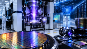
The Dutch semiconductor-equipment giant says it plans to work with major chipmakers to adapt its most advanced High Numerical Aperture Extreme Ultraviolet (High-NA EUV) lithography systems for much larger chips used in AI data centers.
The development could become important for future processors and accelerators designed by companies such as NVIDIA and other major chipmakers, as AI systems demand increasingly powerful silicon.
The key challenge is that today’s High-NA EUV systems can print extremely fine features, but their current mask size limits how large a chip can be manufactured in a single exposure.
ASML’s proposed solution is to move toward larger masks.
ASML Wants High-NA EUV to Handle Much Larger Chips
ASML’s High-NA EUV technology represents the next major step in extreme ultraviolet lithography.
EUV lithography uses extremely short-wavelength light to print incredibly small patterns onto semiconductor wafers. Those patterns eventually become the transistors and interconnects that make modern processors work.
High-NA EUV increases the numerical aperture of the optical system, allowing chipmakers to print finer details with greater precision.
That capability is particularly important as semiconductor manufacturers move toward increasingly dense designs.
But there is a trade-off.
The newest High-NA systems currently use smaller masks than ASML’s existing EUV tools. That creates a limitation when manufacturers want to produce very large chips, including the enormous processors and accelerators increasingly being designed for AI data centers.
ASML now wants to overcome that limitation.
Larger Masks Could Enable Bigger AI Processors
According to Reuters, ASML’s current EUV tools can handle chips measuring up to approximately 800 square millimeters.
Its newer High-NA EUV systems can print smaller features with higher precision, but their existing mask format limits the maximum chip size.
ASML is therefore working toward larger-format masks that could allow High-NA EUV machines to manufacture chips comparable in size to today’s biggest data-center processors.
The goal is not simply to make chips physically larger.
The larger format could allow chip designers to combine more computing resources onto a single piece of silicon while using the improved patterning capabilities of High-NA EUV.
That could become increasingly valuable as AI accelerators continue to grow in complexity.
Why Larger Chips Matter for AI Data Centers
Modern AI systems require enormous amounts of computing power.
Training and serving advanced AI models can involve thousands or even hundreds of thousands of processors operating together inside massive data centers.
One way chip designers increase performance is by adding more computing resources to individual processors.
But larger chips introduce manufacturing challenges.
A larger piece of silicon can provide more space for processing cores, cache, memory interfaces and other components, but producing it efficiently becomes more difficult.
Yield is also an important consideration because a defect anywhere on a large chip can potentially make the entire piece of silicon unusable.
That makes advanced lithography particularly important.
If ASML can combine High-NA EUV’s precision with larger masks, chipmakers could gain another manufacturing option for future large-scale AI processors.
ASML Expects a Major Productivity Improvement
The potential benefit extends beyond simply supporting larger chips.
ASML expects the larger-mask approach could eventually deliver approximately 40% higher system productivity compared with the current approach, according to Reuters.
Higher productivity matters enormously for semiconductor manufacturers.
AI-chip demand is growing rapidly, but chip fabs have limited capacity. If manufacturers can process more wafers or more useful chip patterns in the same amount of time, they can potentially increase output without relying solely on building additional fabrication capacity.
That could become an important competitive advantage as demand for AI infrastructure continues to grow.
NVIDIA Is One of the Potential Beneficiaries
NVIDIA is one of the clearest examples of why ASML’s development matters.
The company has been producing increasingly large and complex processors for AI data centers, while its broader systems increasingly combine GPUs, CPUs, networking and high-bandwidth memory.
ASML’s planned technology is not an NVIDIA-specific product.
Instead, the company is developing manufacturing tools that could eventually be used by multiple chipmakers producing large data-center processors.
That means the potential beneficiaries could include NVIDIA as well as other advanced semiconductor designers.
The development is therefore best understood as infrastructure for the next generation of AI hardware rather than an NVIDIA product announcement.
High-NA EUV Is Already Entering Real Production
ASML’s larger-mask project is a future development, but High-NA EUV itself is no longer purely experimental.
In July 2026, ASML announced that Intel Foundry had entered high-volume manufacturing for a subset of Intel Core Ultra Series 3 processors using its High-NA EUV technology on Intel’s 18A process.
That milestone is significant because it demonstrates that High-NA EUV can move from research and development into actual production.
Intel is currently ahead in deploying the technology.
However, ASML expects adoption across the wider semiconductor industry to take longer.
Reuters reported that high-volume implementation at companies such as TSMC and Samsung has not yet begun. TSMC has projected implementation around 2030, while Samsung and SK Hynix are targeting High-NA EUV for certain DRAM applications by 2028.
The Timeline Shows This Is a Long-Term AI Chip Strategy
ASML does not expect the larger-mask High-NA technology to arrive immediately.
The company plans to demonstrate a pilot line around 2031.
High-volume manufacturing capability is targeted for approximately 2033.
That may sound far away compared with the rapid pace of AI development.
But semiconductor manufacturing operates on a very different timeline.
New lithography platforms require years of engineering, testing, customer qualification and manufacturing optimization before they can become mainstream.
ASML therefore has to anticipate the requirements of chips that may not exist commercially for several years.
Today’s AI accelerators are effectively shaping tomorrow’s semiconductor manufacturing roadmap.
AI Is Driving ASML’s Semiconductor Demand
The AI boom is already having a significant effect on ASML’s business.
In its second-quarter 2026 results, ASML said ongoing AI investment and progress in AI technologies were driving demand for advanced logic and memory chips.
The company reported €9.3 billion in Q2 2026 sales and said it expected full-year 2026 sales of between €43 billion and €45 billion.
ASML also said customer commitments remained strong and planned to increase its 2027 low-NA EUV capacity by around 30% compared with its 2026 level, while investigating additional capacity expansion for 2028.
The message is clear: AI infrastructure investment is influencing not only GPU manufacturers but the equipment companies that make advanced chip production possible.
ASML Sits at a Critical Point in the AI Supply Chain
ASML occupies an unusual position in the semiconductor industry.
It does not design NVIDIA GPUs, Google’s AI accelerators or smartphone processors.
Instead, it builds some of the most sophisticated machines required to manufacture advanced chips.
That makes ASML a critical supplier several steps upstream from the AI products consumers see.
The chain looks roughly like this:
AI models → AI processors → chip fabrication → lithography → ASML equipment
As AI chips become more advanced, the requirements placed on lithography equipment become more demanding.
This gives ASML an important role in the long-term scaling of AI hardware.
Bigger Chips Could Also Increase Manufacturing Complexity
There is an important caveat.
Making chips larger does not automatically make them better or cheaper.
Large dies can create yield challenges, because there is more physical area where manufacturing defects can occur.
Chip designers therefore increasingly use advanced packaging and chiplet architectures to combine multiple pieces of silicon into a larger computing system.
This means ASML’s larger-mask technology will compete with another trend in semiconductor design: breaking complex processors into multiple interconnected components.
Nevertheless, some workloads may benefit from having more functionality integrated directly onto a single die.
The ability to manufacture larger chips with advanced lithography could therefore give designers another option.
The Bigger AI Chip Race Is Moving Into the Factory
The competition surrounding AI is often described as a battle between NVIDIA, AMD, Google, Amazon, Microsoft and other chip designers.
But the deeper competition is happening inside semiconductor factories.
Every improvement in lithography, packaging, memory, interconnects and manufacturing efficiency can influence how quickly the industry can build more powerful AI systems.
ASML’s larger-mask High-NA project is an example of that hidden layer of the AI race.
The company is preparing manufacturing technology for processors that may be significantly larger and more computationally demanding than many chips being produced today.
ASML’s Next Big Bet Could Shape Future AI Hardware
ASML’s plan to adapt High-NA EUV for larger data-center chips is still years away from high-volume production.
The company’s current roadmap points to a pilot line around 2031 and high-volume production capability around 2033.
But the significance of the announcement goes beyond those dates.
AI processors are getting larger, data centers are becoming more compute-intensive, and semiconductor manufacturers need increasingly sophisticated tools to keep scaling performance.
If ASML succeeds in bringing larger-mask High-NA EUV into production, chipmakers could gain a powerful new manufacturing option for future generations of AI processors.
For NVIDIA and other AI-chip designers, that could eventually mean access to more advanced manufacturing capabilities.
For ASML, it represents something even bigger: preparing the machinery that could manufacture the next generation of the AI economy.
Read More:- Qualcomm and Amazon Partner on Custom AI Chips to Challenge NVIDIA in Data Centers
FAQ
What is ASML developing for larger AI chips?
ASML is working with major chipmakers to adapt its High-NA EUV lithography technology for larger chips by developing larger-format masks.
Why does ASML need larger masks?
Current High-NA EUV systems use smaller masks than ASML’s existing EUV tools. Larger masks could allow the technology to manufacture much larger data-center processors.
How could this affect AI chips?
The technology could help manufacturers produce future large AI processors with increasingly dense and advanced transistor designs.
Will NVIDIA use ASML’s new technology?
NVIDIA is one of the companies whose large data-center chips could potentially benefit from the technology, but ASML’s tools are designed for chipmakers broadly rather than exclusively for NVIDIA.
When will ASML’s larger-mask technology be ready?
ASML plans to demonstrate a pilot line around 2031, with high-volume production capability targeted for approximately 2033.
What is High-NA EUV?
High-NA EUV is an advanced semiconductor lithography technology designed to print extremely small and precise patterns onto silicon wafers. The higher numerical aperture improves resolution and process control.
Is High-NA EUV already being used in production?
Yes. ASML announced in July 2026 that Intel Foundry had entered high-volume manufacturing for a subset of Intel Core Ultra Series 3 processors using High-NA EUV on Intel 18A.
Could larger chips improve AI performance?
Larger chips can provide additional physical space for computing resources, although chip size also creates manufacturing and yield challenges. Performance depends on the complete chip architecture, memory system, packaging and software.
How much productivity improvement does ASML expect?
ASML expects the larger-mask approach could eventually improve system productivity by around 40%, according to Reuters.
Why is ASML important to the AI industry?
ASML supplies advanced lithography equipment used by semiconductor manufacturers. Its technology helps chipmakers produce increasingly advanced processors used in AI servers, smartphones, PCs and other devices.